Mystery LCD Module... help!

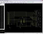
For not being an 'electronics circuit guy', you have bitten off a fair chunk of work (for experienced electronic tinkerers, this stuff is trivial). If you use the 14490, then you don't need to worry about the pullup resistors, they're built into the IC.

You may want to get a protoboard gizmo, the plastic kind with rows of holes containing spring contacts, that you push wires into. That lets you experiment with the wiring without doing any soldering. You'll have to make a 'spread eagled' two row header adapter to go from a standard .1" spacing to the .3" spacing of the protoboard. That's easy, I can give you part numbers of what to buy.

http://rocky.digikey.com/WebLib/Twin Industries/Web Photo/TW-E40-1020.jpg

Once that's working, then you make up a more permanent version using perf-board, that you solder to. There are many styles of perfboard, but here is an example, just so you know what I'm referring to.

http://rocky.digikey.com/WebLib/Vector/Web Photos/8015-1.jpg
Looking for additional LCD resources? Check out our LCD blog for the latest developments in LCD technology.
 

RaduMolasar

New member
Thank you!!!

Will do!

I think I have more than enough tasks now to get my mind busy on this stuff!

Will post results as I get them done...

Thanks for the help!

Best regards,

Mike
 

RaduMolasar

New member
Hello,

I was reading the MC14490 literature and came across two things:

1) Page 1, last paragraph:

"Unused inputs must always be tied to an appropriate logic voltage level (e.g.: either Vss or Vdd)."

Since the LCD module has 5 keys, I'd be left with one unused input. Would I have to wire say, pin 10 (F in) to Pin 16 (Vdd)? Or to Pin 8 (Vss)?

2) Page 5, last paragraph (right hand side):

"However, if an external clock is not available the user can place a small capacitor across the oscillator input and output pins in order to start up an internal clock source..."

Does that mean I have to connect a small capacitor (what value?) to pins 7 (OSC in) and 9 (OSC out)?

USBMicro has already answered and they recommend to use 2 U421 (or U401) modules. Question is: can a single USB header on the motherboard drive both modules? This header originally drives 2 USB chassis mounted ports, so I gather it could... just not sure...

If so, how would the two U421s or U401s need to be wired to be driven from the USB header?

The motherboard is an Asus P5B Deluxe WiFi

Regards,


Mike
 
Would I have to wire say, pin 10 (F in) to Pin 16 (Vdd)? Or to Pin 8 (Vss)?
Theoretically, yes. In actuality, because of the internal pullup to Vdd, it is not important.
Does that mean I have to connect a small capacitor (what value?) to pins 7 (OSC in) and 9 (OSC out)?
You catch on quickly :) . The formula shows that 1.5/Hz = C. So for a clock rate of 6 mS (166 Hz), C would be about .01uF (10000pF). That gives approx 24 mS bounce delay.
USBMicro has already answered and they recommend to use 2 U421 ....
IMHO, using two U421s is too kludgey. I would either use a single U421 along with the 4 bit LCD interface method, OR use a 24 bit USB I/O module, such as the Elexol
http://www.dontronics-shop.com/product.php?productid=16172&cat=320&page=1
 

RaduMolasar

New member
Awesome!!! Way cool!! You are no doubt a very practical man; light years ahead of me already!

I found a PCB layout program called DIP Trace...

I did some initial "fooling around" with it, and here's what I have until now.

The Elexol looks super! I downloaded the datasheet and that's what I'm using for the design.

The wire connections on the schematic look a little deceiving, since I moved the components around with the connections in place (I'll fix them up nicely too during the week).

Haven't got the 30 pin header pinouts yet; that's my current to-do task this week.

Regards,

Mike
 

Attachments

RaduMolasar

New member
LCD pinouts...

Hello,

Finally managed to figure out the pinouts...

I put the PCB against a bright light and it seems to be a 3 layer board, so visual tracing proved quite hard, so I used an ohmmeter and a ton of patience! This is what I got:

Seems this LCD is backlit (looks like internal LEDs -solder leads visible- or something, one each on both ends of the display), but 2 switches (SW2 & SW4) need to be solder closed (or else need to be externally driven). This is just my educated (I think... or hope!) guess.

On pins marked as "unused", I could not find any corresponding link on the PCB.... I didn't try the M5259... Seems kinda strange Pin 3 is unused, so maybe I could've missed something :confused: ...

Anyways, does this pinout make any kinda sense? Any ideas for Pin 3?

I can't quite figure out Pins 1 & 26 vs. Pins 2, 7, 16, 22, 25... I mean to say, 2 grounds? Or maybe not GND, but why NEG (cathode?) on LED, and POS (silk marked + on PCB) on backlight? I'm mixed up here... :confused:


Thanks!

Mike
Code:
30P HDR				PCB
============================================================
1				(LED R/G) - GND
				(BACKLIGHT) - POS (IF SW4 = 1)

2				(HD44780) 23 - GND
				(HD44780) 30 - V5
				(DM7406) 5 - A3
				(DM7406) 7 - GND
				(DM7406) 9 - A4
				(DM7406) 11 - A5
				(DM7406) 13 - A6
				(BACKLIGHT) - GND (IF SW2 = 1)
				(BUTTONS) - COMMON

3				UNUSED

4				(HD44780) 36 - RS
5				(HD44780) 37 - RW
6				(HD44780) 38 - E

7				(HD44780) 23 - GND
				(HD44780) 30 - V5
				(DM7406) 5 - A3
				(DM7406) 7 - GND
				(DM7406) 9 - A4
				(DM7406) 11 - A5
				(DM7406) 13 - A6
				(BACKLIGHT) - GND (IF SW2 = 1)
				(BUTTONS) - COMMON

8				(HD44780) 39 - DB0
9				(HD44780) 40 - DB1
10				(HD44780) 41 - DB2
11				(HD44780) 42 - DB3
12				(HD44780) 43 - DB4
13				(HD44780) 44 - DB5
14				(HD44780) 45 - DB6
15				(HD44780) 46 - DB7

16				(HD44780) 23 - GND
				(HD44780) 30 - V5
				(DM7406) 5 - A3
				(DM7406) 7 - GND
				(DM7406) 9 - A4
				(DM7406) 11 - A5
				(DM7406) 13 - A6
				(BACKLIGHT) - GND (IF SW2 = 1)
				(BUTTONS) - COMMON

17				UP BUTTON
18				DOWN BUTTON
19				RIGHT BUTTON
20				MENU BUTTON
21				OK BUTTON

22				(HD44780) 23 - GND
				(HD44780) 30 - V5
				(DM7406) 5 - A3
				(DM7406) 7 - GND
				(DM7406) 9 - A4
				(DM7406) 11 - A5
				(DM7406) 13 - A6
				(BACKLIGHT) - GND (IF SW2 = 1)
				(BUTTONS) - COMMON

23				(DM7406) 3 - A2
24				(DM7406) 1 - A1

25				(HD44780) 23 - GND
				(HD44780) 30 - V5
				(DM7406) 5 - A3
				(DM7406) 7 - GND
				(DM7406) 9 - A4
				(DM7406) 11 - A5
				(DM7406) 13 - A6
				(BACKLIGHT) - GND (IF SW2 = 1)
				(BUTTONS) - COMMON

26				(LED R/G) - GND
				(BACKLIGHT) - POS (IF SW4 = 1)

27				UNUSED
28				UNUSED
29				UNUSED
30				UNUSED

============================================================

LED R				(DM7406) 2 - Y1
LED G				(DM7406) 4 - Y2
 

Attachments

Last edited:
Seems reasonable to me.

I think pins 1 & 26 are Vcc (+5v). Are these pins connected to HD44780 pin 33? If not, then is pin 33 connected to any header pin? I believe the LED has a common anode (center lead to +5), and 2 cathodes (R & G).

As for all the GND pins, that's fine. V5 is the signal that might have been connected to header pin 3. Since it is grounded, then Vo is fixed at 0v, which probably gives adequate (or slightly high) contrast. I assume that R1,R2,R4,R5 form the V1~V5 divider chain.

Are you sure header pin 3 doesn't connect to anything? If not, no big deal.

Looks like you are ready to roll. Put 5v on pin 1 and GND on pin 2, and you should get the top row of cells all dark on the screen. If so, then hook it up to your USB thing, and give it a try.
 

RaduMolasar

New member
Hello,

I marked Pins 1 & 26 as (LED R/G) - GND because it actually goes to the center lead, so I assumed it was the cathode (-), but I do believe you're right. It does look like a common anode (+), because else the (BACKLIGHT) - POS (IF SW4 = 1) would not make sense, and THAT IS marked (+) on the board.

I'll do the following tonight:

Double check HDR30 Pin 1 to HD44780 Pin 33.

Double check HD44780 Pin 33 to any HDR30 Pins

I assume that R1,R2,R4,R5 form the V1~V5 divider chain.
Gee... I see the resistors on the PCB, but no idea what they're for. Divider chain? Wass that? :confused:

Other question:

I suppose DB0~DB7 go to USB lines, so to say. What about RS, RW & E? Them too?

I will try to see if HDR30 Pin 3 goes to SW1. Maybe that's why it doesn't show up to any of the HD44780 pins... just guessing...

Isn't HDR30 Pin 1 suppose to go someplace else too? I just see it going to the LEDs... :confused:

Will post results tomorrow.

Thanks!

Mike
 
Last edited:
I suppose DB0~DB7 go to USB lines, so to say. What about RS, RW & E? Them too?
Yes, them too, but only if you want the display to work.
Isn't HDR30 Pin 1 suppose to go someplace else too? I just see it going to the LEDs...
I expect it would connect to HD44780 pin 33, M5259 pin 43, and DM7406 pin 14, else those ICs would have no power.
 

RaduMolasar

New member
Yes, them too, but only if you want the display to work.
:D Since that is a big YES, that makes DB0~DB7 + RS, RW & E go to 11 USB lines...

Add 5 buttons... 16 lines...

R/G LED... 18 lines...

Any other lines I need to consider?

You're right; I double-checked. Pin 1 goes to (HD44780) Pin 33 & (DM7406) Pin 14... how could I miss that? :confused:

I attached an updated pinout list.

I didn't check the M5259, but your conclusion must necessarily be correct.

Pin 3 of the HDR30 is unused. I triple-checked it. Not used at all (I did not check the M5259, though). At least it is for sure not used on the HD44780, DM7406, LEDs, etc.

I also checked out the R/G LED. I compared it to this image:

http://en.wikipedia.org/wiki/Image:+-_of_LED.svg

The center LED lead does in fact look like a small trumpet or funnel, somewhat matching the (+) lead of the image (if you were to oppositely mirror -double- it); the R/G leads do look like the (-) lead of the image, which also confirms your theory that the anode is common.

I'll update my schematic; I've seen services which will create a PCB board out of a design one provides. I guess I'll go this route for the final piece.

Regards,

Mike
 

Attachments

Last edited:
Seems like you've accounted for all the signals. So, you're not going to hook it up temporarily with a breadboard, to see if it even works, before committing to a pcb? Your design may have a simple error, or you may discover something during software development that would require a circuit change. Did you remember to sprinkle in a few bypass caps?
 

RaduMolasar

New member
Hello,

No sir, I will indeed try out the design on an experimenter's breadboard. I meant to say that the ultimate final piece will be a PCB.

Did you remember to sprinkle in a few bypass caps?
:eek: Huh? What's that? :confused:


Regards,

Mike
 

RaduMolasar

New member
Hello...

One question:

On an earlier post, I wrote:

I was reading the MC14490 literature and came across two things:

1) Page 1, last paragraph:

"Unused inputs must always be tied to an appropriate logic voltage level (e.g.: either Vss or Vdd)."

Since the LCD module has 5 keys, I'd be left with one unused input. Would I have to wire say, pin 10 (F in) to Pin 16 (Vdd)? Or to Pin 8 (Vss)?
You said it was not really important... so, should I definitely leave it untied, or maybe it's best to wire it, just to be sure?

If wired, where to? Vss or Vdd?

Excuse the question. I just kind of felt unsure of what to do.

BTW, here's an updated schematic. Does it seem ok?

Thanks!

Mike
 

Attachments

Last edited:
Schematic and pcb layout look nice. One comment: bypass caps should be close to the pin they are bypassing. I would swap the location of C1 and C2, so that each has shorter traces to U1. Does that pcb layout package allow for thermal reliefs for pads in a plane (pad is isolated from plane with radial spokes)? If not, you'll have trouble soldering those holes, as the plane makes a good heat sink.

As for the unused input to the 14490, it really doesn't matter, since this particular IC has built-in pullups on the inputs. Its funny that the warning is given in the data sheet for a chip that doesn't need it.
 

RaduMolasar

New member
Hello,


Yes, this package does allow isolated pads for copper pours, etc (I found that out once you mentioned it). Take a look at the images (I swapped C1 and C2 too).

Seems DIPTrace is a full blown pro PCB package which one can download for free (only limitation is the pin count on freeware version), or purchase a license to "unlock" ("unleash" I think is a better term!) the freeware and get more pin counts. Other than that, there is no limitation.

The autorouter did have problems routing the board (or maybe I just didn't know how to set adjustments correctly), so I tried Electra Autorouter Demo (which is partnered with DipTrace) and it did a wonderful job very fast!

I'm not really into PCB electronics (I'm a software developer), but this is quite exciting and very fun!

Thanks for the help!!! I'll keep on postin' as I make more progress!

Thanks again and best regards!

Mike
 

Attachments

One thing about the copper pour planes is sometimes you can get into a situation where islands are isolated from the other parts of the same net. I see you've got that covered by traces on the other side. Another thing about autorouters is they aren't smart enough to route traces so that the copper pour forms the fewest islands. For example, the traces between C2 and U1 split the ground plane, causing the connection from the ground lead of C2 to the ground pin of U1 to have a long skinny trace path. It should't matter in this circuit, but by moving C2 and 3 traces, that path could be made into 1 plane island. But, hey, don't mind my criticisms, I'm just fussy about optimizing layouts. I always hand route the final touchups. For a non-electrical person, you've done a good job.

But the real question is ... (drum roll) ... have you breadboarded the hookup to the LCD, written a piece of test code, and made sure the circuit actually works?
 

RaduMolasar

New member
Hi there!


Constructive criticism is always welcome! Perfectionists are my kinda people! I'm like this too most of the time, but... You're right. I miss those details because I don't know what to look for, and am not familiar with effects and outcomes.

Of the breadboard and stuff, I haven't yet built it. I just ordered 2 debouncer chips, and will order the Elexol interface sometime next week (maybe this weekend). I haven't dismissed the importance of testing first, building later. I just got carried away with this PCB proggy.

I searched the net and it seems the only thing I'll run into trouble getting is the high-density 30 pin header. Can't seem to find it no place...

Thanks again for your comments and thoughts. They are very much appreciated and very valuable too!!

Kind regards,

Mike
 
Top