Samsung S6B0721 initialization

cleonard99999

New member
Hi-
Trying to get a Samsung S6B0721 graphics LCD driver initialized, but not having any luck. I believe this part uses the KS0713 chipset, although I'm not 100% sure.

After powerup, I leave RESETB low for about 1.5ms, pull it high, set RS and CS1B low, then have a micro send the following commands via a serial connection:

ADC Select (0xA1)
SHL Select (0xC8)
LCD Bias Select (0xA2 = 1/7 bias, 1/65 duty)
Voltage Converter On (0x2C)
(wait 2ms)
Voltage Regulator On (0x2E)
(wait 2ms)
Voltage Follower On (0x2F)

Regulator Resistor Select (0x26 for V0=5.29*Vev=8.51V)
Set Reference Voltage Mode (0x81)
Set Reference Voltage Level (0x04 for Vev=0.803*Vref=1.61V)
(wait 2ms)

Turn on display (0xAF)
Turn on all pixels (0xA4)

This setup has no effect whatsoever. I've tried running with breakpoints after every single command, so I know time between each of these commands isn't the cause. Is there a better setup routine? I'm just doing what the datasheet suggests.

The LCD is 96x64 dots and supposedly runs at 8.5 V, 1/7-bias, and 1/65-duty. I should probably add that I'm a software engineer who knows little about LCDs except for what was is the datasheet for this part-this is new territory for me. ANY help would be very very much appreciated.
Looking for additional LCD resources? Check out our LCD blog for the latest developments in LCD technology.
 
Can you supply any more info about the physical display (model, mfgr)? Is the charge pump circuitry integrated (like the CFAX series), or did you wire it yourself? Can you measure V0 and Vout? How are the other control inputs wired, pulled up/down or left floating?
 

cleonard99999

New member
Thanks for the replys-
The LCD is a chip-on-glass style manufactured by Smart Good Enterprises (I don't have a model number right now, since I left the data sheet at work).
All other control pins are internal to the LCD/IC package; I'm presuming they're pulled up/down internally.
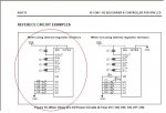
The charge-pump circuitry is not integrated and is wired externally. I attached the reference circuit i used-it's the circled diagram on the left. i used all 1 uF capacitors.
 

Attachments

So you are using a 4x boost circuit with 3.3v Vdd. The question remains: can you measure V0 and Vout?

This will tell whether your LCD voltage is "reasonable", and that the init procedure is working, although your data sheet should tell what voltage the display panel requires. If its 8.5 volts, as you mention, then the 4x boost seems excessive.
 

cleonard99999

New member
OK, I just tried measuring V0 and Vout: Vout = 2V and V0 = 0V.
These values never change, so I'm guessing there's either the LCD doesn't see my serial commands or there's a problem with the LCD driver itself (I've already switched displays once, but I suppose it's possible both are bad).
The serial data looks good (3V, 56us clock cycle-slowed down to be safe, data going in msb->lsb), I'll keep checking for anything else amiss.
 
As a troublshooting aid, you could use the "external" lcd power supply method shown in figure 19 of the data sheet. You can try a 9 volt battery just to see if there is data on the screen.

In my displays, the Vout is about -9.5 volts (ref to Vss), and V0 is about -4.7 volts for good contrast. The V0-V4 values will depend on your register settings (resistor ratio, and electronic 'volume').

Mine: V0 is -4.7, V1 is -3.6, V2 is -2.5, V3 is +2.6, V4 is +3.9.

Are you setting the RS input (during DB0 bit) correctly? How are the other control signals controlled (what states)?
 

cleonard99999

New member
The external power supply's a good idea-I'll try that. I don't quite follow you about RS during DB0, although I noticed Figure 3 in the datasheet seems to imply a transistion on RS during DB0. Is this referring to the state of RS for the next byte? Currently I pull RS low before sending data and keep it low (since I'm not sending any display data yet).
As for other control pins, serial clock/data, RESETB, CS1B, and RS are the only external control lines for this lcd module. I set RESETB high and CS1B low after setting RESETB low for ~50us to initialize the driver.
 
If you try the external battery connected to Vout, be sure to keep the Vc bit low in the power control register (i.e. use 0x2B instead of 0x2F) in your init sequence.

Figure 3 shows that the RS bit must be at the desired state during the clock transition for DB0, and is irrelevant at other times. To simplify the code, I'd just set it high or low at the start of each byte, and leave it the same for all 8 bits.

You show 'all pixels on' as 0xA4, but it should be 0xA5, so you would be setting it to 'normal', which would show no pixels.

Also, try changing SHL select from 0xC8 to 0xC0. Since the controller is 135 columns, and the screen is only 64 columns, maybe the 'active' columns are off-screen (not likely, but can't hurt to try). Same for ADC select, try 0xA0 instead of 0xA1.
 

cleonard99999

New member
My mistake, I meant to say 0xA5 for "all pixels on".

Haven't had any more luck, but did have another question-the setup procedure in Figure 27 says ResetB should be held low when Vdd is turned on; is this critical? Right now, I apply a reset, but not until after turning on power. I tried putting a pull-down resistor on that pin to be safe, but apparently the micro I'm using has pull-ups on all i/o (which I haven't yet found a way to get rid of). Thanks
 

cleonard99999

New member
OK, got it now-just a problem with the micro's serial bus, was clocking in an extra bit before the init data, so all the data was off by one bit. Thanks for the help though
 
Top